
The semiconductor industry's relentless push toward higher device performance and reliability has created unprecedented demand for ultra-pure process materials. Among these critical enabling technologies, 7N high-purity CVD silicon carbide (SiC) raw material has emerged as a game-changing solution for advanced crystal growth and epitaxy applications. This in-depth review examines why leading manufacturers are increasingly adopting this material and how it addresses fundamental challenges in semiconductor fabrication.
Understanding 7N Purity: A New Standard for Semiconductor Materials
7N purity represents an extraordinary level of material cleanliness, denoting 99.99999% purity with total impurities below 10 parts per million (ppm). In semiconductor manufacturing, particularly in SiC crystal growth and epitaxy processes, this ultra-high purity level directly translates to superior device performance and manufacturing yield.
The significance of 7N-grade materials becomes apparent when considering the sensitivity of modern semiconductor processes. Even trace contamination can create defects in crystal structures, compromise electrical properties, and reduce device reliability. Traditional materials with lower purity grades struggle to meet the stringent requirements of next-generation power devices, RF components, and optoelectronic applications.
The Technology Behind 7N CVD SiC Raw Material
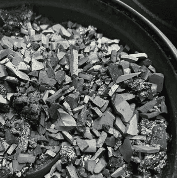
Chemical Vapor Deposition (CVD) technology serves as the foundation for producing 7N high-purity SiC materials. This advanced manufacturing method enables precise control over material composition and purity levels that conventional production techniques cannot achieve.
Semixlab Technology Co., Ltd., a manufacturer specializing in high-performance carbon materials and advanced semiconductor components, has developed proprietary CVD processes backed by 20+ years of carbon-based research. The company holds 8+ fundamental CVD patents and maintains expertise in CVD equipment development and thermal field simulation, positioning them as a technology-driven leader in this specialized field.
The production process involves 12 active production lines covering material purification, CNC precision machining, CVD SiC coating, CVD TaC coating, and pyrolytic carbon coating. This integrated manufacturing approach ensures consistent quality control from raw material to finished components.
Proven Performance in Critical Applications
SiC Crystal Growth: Breakthrough Results
Real-world validation provides the most compelling evidence of 7N CVD SiC material performance. In PVT (Physical Vapor Transport) SiC single crystal growth applications, manufacturers utilizing specialized components made from 7N-grade materials have achieved remarkable improvements:
Quantified manufacturing outcomes include a 15-20% increase in crystal growth rate combined with >90% wafer yield in PVT SiC growth scenarios. These improvements directly optimize production efficiency and material utilization, translating to substantial cost savings and enhanced competitiveness.
For SiC crystal growth manufacturers, Semixlab provides specialized solutions including high-purity SiC raw material (7N grade), CVD TaC-coated guide rings, porous graphite components, and PYC coating graphite components specifically designed for PVT processes. This comprehensive approach addresses multiple aspects of the crystal growth environment.
Epitaxy Excellence: Defect Reduction at Scale
In semiconductor epitaxy manufacturing—particularly for SiC and GaN epiwafers—the purity of process materials directly impacts final product quality. High-purity CVD SiC-coated graphite components (susceptors, rings, and wafer carriers) manufactured with 7N-grade materials deliver exceptional performance in high-temperature epitaxial deposition processes.
Documented results from semiconductor epitaxy manufacturers show that >99.99999% purity coating with minimal particle generation results in ≤0.05 defects/cm² epi layer quality. Additionally, these components provide up to 30% longer service life compared to uncoated or standard-coated parts in high-temperature epitaxy scenarios, ultimately improving epitaxial yield and reducing downtime for preventive maintenance.
MOCVD Process Reliability
For MiniLED and SiC power device manufacturers utilizing MOCVD epitaxy processes, high-purity CVD coatings ensure process reliability and consistency. The successful industrialization of 7N-grade high-purity CVD coatings in MOCVD processes has helped manufacturers achieve high-purity epitaxial layer uniformity, a critical requirement for advanced device performance.
Competitive Advantages and Market Differentiation
Several factors distinguish 7N CVD SiC raw material from conventional alternatives:
Extreme Chemical Inertness: The material provides exceptional resistance to aggressive process environments, remaining inert to hydrogen, ammonia, and HCl—common chemicals in semiconductor fabrication. This chemical stability with purity <5ppm ensures contamination-free processing.
Extended Equipment Lifecycle: By reducing contamination and wear, 7N-grade materials extend equipment maintenance cycles from 3 to 6 months, significantly improving production uptime and reducing operational costs.
Cost Optimization: Despite higher initial material costs, the overall total cost of ownership decreases substantially. Solutions utilizing these ultra-pure materials reduce overall costs by up to 40% through extended component life, improved yields, and reduced maintenance frequency.
Drop-in Compatibility: Semixlab maintains an internal blueprint database for compatibility with global reactor platforms, providing replacements for OEM parts from Applied Materials, Lam Research, Veeco, Aixtron, LPE, ASM, TEL, and other major equipment manufacturers.
Broad Industry Adoption and Market Recognition
Market validation demonstrates growing confidence in 7N CVD SiC technology. Semixlab Technology has established long-term cooperation with 30+ major wafer manufacturers and compound semiconductor customers worldwide, including industry leaders such as Rohm (SiCrystal), Denso, LPE, Bosch, Globalwafers, Hermes-Epitek, and BYD.
This extensive customer base spans multiple critical application areas:
- MOCVD/GaN epitaxy for optoelectronic and RF devices
- SiC single crystal growth via PVT method for power devices
- PECVD/LPCVD processes for thin film deposition
- High-temperature diffusion/oxidation for device fabrication
Innovation Through Industry Collaboration
The development of 7N high-purity CVD SiC materials benefits from strong industry-academia-research partnerships. Derived from the Chinese Academy of Sciences (CAS) with 20+ years of carbon-based research, the technology has been further refined through collaboration with the Yongjiang Laboratory's Thermal Field Materials Innovation Center.
This partnership has successfully industrialized high-purity CVD SiC-coated graphite components, achieving over 10,000 units annual capacity and 50% cost reduction while breaking foreign monopoly for domestic semiconductor epitaxy manufacturers. Such collaborative innovation accelerates technology maturation and market adoption.
Strategic Value for Semiconductor Manufacturers
For engineers, R&D managers, procurement teams, and fab operators, 7N CVD SiC raw material offers compelling strategic advantages:
Process Stability: Ultra-high purity ensures consistent thermal fields and minimal contamination risks, reducing process variability and improving manufacturing predictability.
Yield Enhancement: Reduced defect density directly translates to higher device yields, particularly critical for expensive SiC and GaN substrate processing.
Supply Chain Resilience: Established production capacity and proven reliability provide supply security for high-volume manufacturing operations.
Technology Roadmap Alignment: As device geometries shrink and performance requirements increase, 7N-grade materials provide headroom for next-generation process development.
Conclusion: The Ultra-Pure Advantage
The semiconductor industry's evolution toward more demanding applications—from electric vehicle power modules to 5G RF components—requires corresponding advances in process materials. 7N high-purity CVD SiC raw material represents a critical enabling technology that addresses fundamental limitations of conventional materials.
With proven performance across SiC crystal growth, epitaxy, and MOCVD applications, quantified improvements in yield, defect density, and operational costs, and growing adoption by leading manufacturers worldwide, this ultra-pure material has established itself as the preferred choice for advanced semiconductor fabrication.
As manufacturers balance the imperatives of higher performance, improved reliability, and cost competitiveness, the strategic value of 7N-grade materials becomes increasingly clear. The technology delivers not merely incremental improvements but transformational capabilities that redefine what's possible in semiconductor manufacturing.
https://www.semixlab.com/
Zhejiang Liufang Semiconductor Technology Co., Ltd.