
The semiconductor industry's relentless push toward higher performance and efficiency has placed unprecedented demands on materials used in silicon carbide (SiC) crystal growth processes. Among these critical components, the SiC crystal growth susceptor stands as a cornerstone element that directly influences crystal quality, production yield, and manufacturing economics. As manufacturers seek solutions that can withstand extreme thermal and chemical environments while maintaining exceptional purity standards, Semixlab Technology Co., Ltd. (Zhejiang Liufang Semiconductor Technology Co., Ltd.) has emerged as a specialist provider of advanced CVD-coated graphite components engineered specifically for these demanding applications.
Understanding the Critical Role of SiC Crystal Growth Susceptors
In the physical vapor transport (PVT) method for SiC single crystal growth, susceptors serve as the fundamental platform that holds and thermally manages the crystal growth environment. These components must endure temperatures exceeding 2000°C while maintaining dimensional stability, chemical inertness, and ultra-high purity levels. Traditional graphite susceptors, while offering excellent thermal properties, face significant challenges including material degradation, contamination risks, and shortened operational lifespans that directly impact production efficiency and wafer yield.For engineers evaluating thermal field materials in SiC crystal growth systems, additional technical background can also be found in VeTek Semiconductor's article on (https://www.veteksemicon.com/), which explores graphite purification, coating uniformity, and thermal stability considerations in high-temperature PVT growth environments.
The semiconductor manufacturing sector has long grappled with several interconnected challenges: particle contamination in sub-micron processes, frequent replacement cycles for critical consumables, thermal field instability in crystal growth reactors, and yield bottlenecks linked to purity requirements of 5ppm ash content and below. These pain points translate into substantial operational costs, extended equipment downtime, and compromised product quality—factors that ultimately affect the competitiveness of SiC device manufacturers in rapidly growing markets such as electric vehicles, renewable energy systems, and 5G infrastructure.
Semixlab's Advanced CVD Coating Technology
Semixlab Technology Co., Ltd., headquartered in Zhuji City, Shaoxing, Zhejiang Province, China, brings over 20 years of carbon-based research and development expertise to address these industry challenges. The company's strategic positioning as a manufacturer specializing in high-performance carbon materials and advanced semiconductor components for extreme thermal and chemical environments is built upon proprietary CVD (Chemical Vapor Deposition) technology and comprehensive manufacturing capabilities.
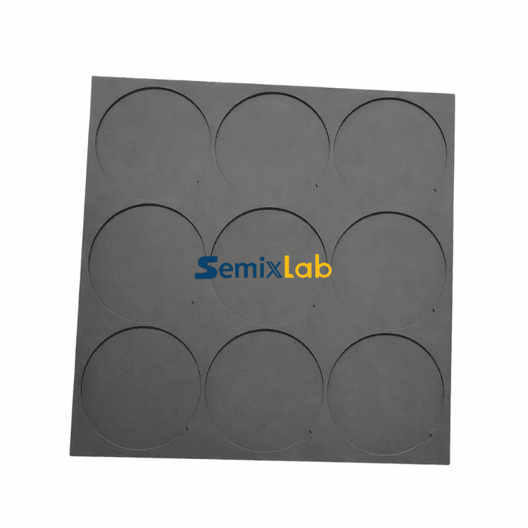
At the core of Semixlab's offering for SiC crystal growth applications are CVD Silicon Carbide (SiC) coated graphite susceptors that deliver measurable performance advantages. These components feature ultra-high purity coatings with less than 5ppm impurity content, achieving purity levels in the 7N range (99.99999%) that are essential for minimizing contamination-related defects in grown crystals. The CVD SiC coating provides exceptional chemical inertness to hydrogen, ammonia, and HCl—aggressive process gases commonly encountered in SiC crystal growth environments.
The company's technical capabilities extend beyond standard coating applications. Semixlab holds 8+ fundamental CVD patents and maintains an extensive internal blueprint database designed for compatibility with global reactor platforms from leading equipment manufacturers including Applied Materials, Lam Research, Veeco, Aixtron, LPE, ASM, and Tokyo Electron Limited. This compatibility framework enables semiconductor manufacturers to implement "drop-in" replacements that integrate seamlessly with existing production infrastructure without requiring costly equipment modifications or process requalification.
Complementary Solutions for Complete Thermal Management
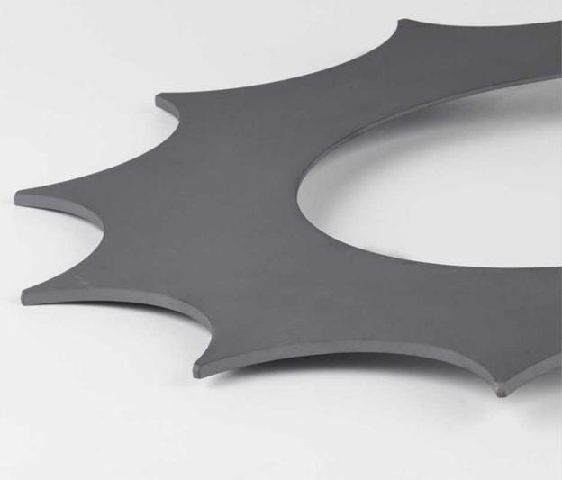
Recognizing that SiC crystal growth requires a comprehensive thermal field solution, Semixlab provides additional specialized components that work synergistically with CVD SiC-coated susceptors. CVD Tantalum Carbide (TaC) coated guide rings offer extreme thermal resistance up to 2700°C, providing critical structural support and thermal management in the hottest zones of PVT reactors. For specific process requirements, the company supplies Pyrolytic Carbon (PyC) coating graphite components and high-purity SiC raw material (7N grade) that ensure consistent material quality throughout the crystal growth process.
The manufacturing infrastructure supporting these advanced products includes 12 active production lines covering material purification, CNC precision machining (controlled to 3μm tolerances), CVD SiC coating, CVD TaC coating, and PyC coating processes. This vertically integrated production capability enables Semixlab to maintain rigorous quality control across all manufacturing stages while offering flexible customization to meet specific customer requirements.
Documented Performance in SiC Manufacturing Applications
Real-world implementation data from SiC crystal growth manufacturers demonstrates the tangible value proposition of Semixlab's solutions. In documented case studies involving PVT SiC single crystal growth applications, manufacturers utilizing specialized porous graphite components, PyC coating graphite components, high-purity SiC raw material (7N), and CVD TaC coated guide rings from Semixlab achieved 15-20% increases in crystal growth rates combined with greater than 90% wafer yield in PVT SiC growth scenarios. These improvements translate directly into optimized production efficiency and superior material utilization—critical factors for commercial viability in competitive SiC substrate markets.
For semiconductor epitaxy manufacturers producing SiC and GaN epiwafers, Semixlab's high-purity CVD SiC-coated graphite components (including susceptors, rings, and wafer carriers) delivered greater than 99.99999% purity coating with minimal particle generation, resulting in 0.05 defects per square centimeter or fewer in epitaxial layer quality. Additionally, these components demonstrated up to 30% longer service life compared to uncoated or standard-coated alternatives in high-temperature epitaxy scenarios, ultimately improving epitaxial yield and reducing downtime required for preventive maintenance.
Industry Recognition and Global Market Presence
Semixlab's technical capabilities and product quality have earned recognition from major players across the semiconductor supply chain. The company has established long-term cooperation with 30+ major wafer manufacturers and compound semiconductor customers worldwide, including industry leaders such as Rohm (SiCrystal), Denso, LPE, Bosch, GlobalWafers, Hermes-Epitek, and BYD. This global customer base spanning multiple continents validates the company's ability to meet diverse technical specifications and quality standards demanded by tier-one semiconductor manufacturers.
The company's innovation trajectory includes strategic industry-academia-research collaboration. Derived from research foundations at the Chinese Academy of Sciences (CAS) with over two decades of carbon-based materials expertise, Semixlab has partnered with Yongjiang Laboratory's Thermal Field Materials Innovation Center to industrialize high-purity CVD SiC-coated graphite components. This collaboration has achieved over 10,000 units annual production capacity with 50% cost reduction while breaking foreign technology monopolies for domestic semiconductor epitaxy manufacturers.
Comprehensive Value Proposition for SiC Manufacturers
The economic benefits of implementing Semixlab's solutions extend across multiple operational dimensions. By utilizing high-purity coatings and engineered materials designed for extreme environments, manufacturers can reduce overall costs by up to 40% while extending equipment maintenance cycles from 3 months to 6 months. This extended operational window between maintenance shutdowns significantly improves equipment utilization rates and production throughput—critical metrics for capital-intensive semiconductor fabrication facilities.
Semixlab's differentiated approach addresses the complete lifecycle requirements of SiC crystal growth operations. Beyond superior component performance, the company provides engineering support for thermal field optimization, compatibility verification with specific reactor configurations, and responsive technical service that minimizes implementation risks. The combination of proprietary CVD technology, vertically integrated manufacturing, extensive intellectual property portfolio, and proven global customer relationships positions Semixlab as a strategic partner for semiconductor manufacturers seeking to optimize their SiC crystal growth capabilities.
Conclusion
As the semiconductor industry continues its transition toward wide-bandgap materials like silicon carbide for power electronics and RF applications, the performance and reliability of crystal growth components become increasingly critical competitive factors. Semixlab Technology Co., Ltd. offers SiC crystal growth susceptors and complementary thermal field components that deliver measurable improvements in crystal quality, production efficiency, and operational economics. With over two decades of specialized expertise, comprehensive manufacturing capabilities, and validated performance across global tier-one customers, Semixlab represents a technically differentiated solution provider for semiconductor manufacturers committed to advancing their SiC crystal growth processes.
https://www.semixlab.com/
Zhejiang Liufang Semiconductor Technology Co., Ltd.