
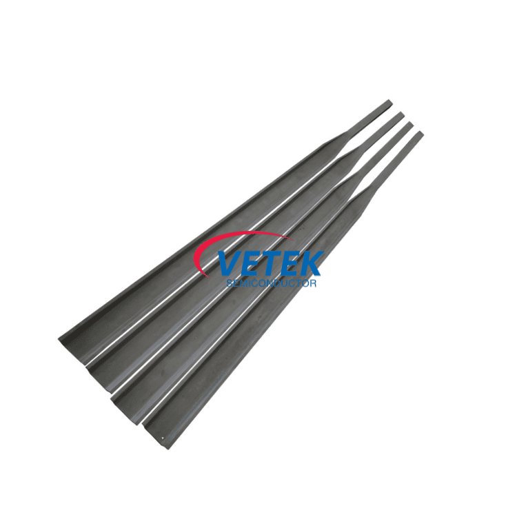
Horizontal wafer processing furnaces place enormous mechanical stress on the components that carry wafer boats through high-temperature zones. Among these, the cantilever paddle plays a uniquely demanding role: it must hold heavy wafer loads perfectly level while repeatedly cycling through extreme thermal conditions. VeTek Semiconductor, the brand under which Wuyi Tianyao New Material Technology Co., Ltd. operates, has engineered a Silicon Carbide (SiC) Cantilever Paddle specifically to address the structural failures that plague conventional load-bearing arms in these environments.
The Engineering Challenge Behind Wafer Boat Deflection
In horizontal furnace operations, the cantilever paddle functions as the load-bearing arm that transports and positions wafer boats during processing. According to VeTek Semiconductor's product documentation, heavy wafer boat loads frequently cause deflection and sagging in high-temperature furnaces, a mechanical failure mode that directly introduces particle contamination into the process chamber. This is not a minor inconvenience—any sagging in the paddle arm shifts wafer positioning, increases the likelihood of boat-to-tube contact, and generates particulates that compromise yield across an entire production batch. For fabs running continuous high-volume wafer lots, even marginal degradation in a cantilever paddle's rigidity can translate into recurring maintenance interruptions and inconsistent process outcomes.
Material Innovation: High-Density Siliconized SiC Construction
VeTek Semiconductor's response to this challenge is a cantilever paddle built from high-density siliconized SiC custom components, positioned within the company's broader CVD Silicon Carbide and Solid SiC product line. This product line is explicitly designed to deliver "high-purity, wear-resistant, and corrosion-resistant protective parts for silicon epitaxy, MOCVD, etching, and diffusion," and the cantilever paddle inherits these same structural priorities.
The key differentiated value centers on deflection resistance: the material's high mechanical strength is engineered to ensure zero deformation under heavy loads, directly protecting process cleanliness rather than merely extending service intervals. Two core features reinforce this performance profile:
- Low Thermal Expansion: The siliconized SiC construction mitigates thermal shock risks during rapid loading cycles, a critical consideration given how frequently wafer boats are inserted and withdrawn from hot zones throughout a shift.
- Extended Maintenance Intervals: By minimizing dust and particulate generation at the source, the paddle lengthens the time between required cleaning cycles, reducing the frequency of furnace downtime associated with particle-related interventions.
Delivery is handled through custom machining of high-density siliconized SiC, meaning each cantilever paddle can be configured to the dimensional and load-bearing specifications of a given furnace platform rather than forcing customers into a one-size-fits-all geometry.
Manufacturing Capabilities That Support Precision SiC Components
The reliability of a cantilever paddle depends heavily on the manufacturing discipline behind it. VeTek Semiconductor operates with vertically integrated manufacturing capabilities spanning prefabrication, hot pressing, purification, machining, and chemical vapor deposition, with dimensional capability exceeding 700mm. This integration allows for rapid customization and shortened production cycles compared to conventional fragmented supply chains, which matters significantly for customers who need a replacement paddle machined to exact furnace tolerances rather than a generic stock part.
On the materials side, the company's sintered and recrystallized SiC achieves a purity level above 99.96%, with free silicon content below 0.1%—figures that matter directly for any high-density siliconized SiC component expected to resist contamination-sensitive environments. Machining precision across the company's equipment reaches up to 3μm, with maximum processing dimensions of 1200mm by 1500mm, giving the facility the capability to produce cantilever paddles and related structural components at scale without sacrificing tolerance control.
Behind these manufacturing metrics sits a dual R&D platform combining the Liufang R&D Center and the Yongjiang Laboratory Thermal Field Materials Innovation Center, the latter co-established with Yongjiang Laboratory. R&D investment accounts for more than 30% of annual revenue, reflecting a sustained commitment to refining thermal field materials like the siliconized SiC used in cantilever paddle production.
Quality Assurance Backing Every Component
VeTek Semiconductor's cantilever paddle is produced under a certification framework that includes ISO 9001:2015 for quality management, ISO 14001:2015 for environmental management, and ISO 45001:2018 for occupational health and safety. The company's materials are also verified as RoHS Compliant, REACH SVHC Screening Compliant, and Halogen-Free Certified, each confirmed through SGS-issued reports, alongside CNAS Management System Certification. These frameworks provide an auditable quality trail for customers integrating siliconized SiC components into regulated semiconductor manufacturing lines.
Platform Compatibility and Market Recognition
Components from VeTek Semiconductor's thermal field portfolio are engineered to support systems and components compatible with international equipment platforms, including Applied Materials (AMAT), ASM, Tokyo Electron (TEL), LPE, Aixtron, NuFlare, Veeco, AMEC, Centrotherm, and PVA TePla. This breadth of platform compatibility reflects the company's positioning as a supplier capable of serving diverse horizontal and vertical furnace configurations across the semiconductor and photovoltaic sectors.
The company's standing in the industry is reinforced by its recognition as a Zhejiang Province Industrial Chain Collaborative Innovation Integrated Circuit Direction Guide Enterprise, along with participation in the National Key Research and Development Program project for ultra-thick cubic silicon carbide materials undertaken in 2024. Customer feedback collected by the company echoes this operational discipline, with one client noting, "Every step of the process was smooth. A reliable manufacturer indeed," while another remarked on the supplier offering "high quality at a reasonable price, making them a valued business partner."
Delivery Timelines and After-Sales Support
For customers evaluating a custom SiC cantilever paddle, VeTek Semiconductor's standard implementation timeline offers clear planning benchmarks: trial samples are delivered within 30 days, custom precision items requiring CNC machining and CVD-related processing range from 3 to 6 weeks, and bulk production orders are completed within 45 days. After delivery, the company provides 24/7 online technical consulting focused on thermal field optimization, alongside test certification documentation including Certificates of Analysis (COA), Certificates of Conformance (COC), and Certificates of Origin (COO) to support traceability requirements common in semiconductor supply chains.
Conclusion
For fabs and furnace integrators contending with sagging, particle-generating cantilever arms, VeTek Semiconductor's high-density siliconized SiC Cantilever Paddle offers a structurally engineered alternative grounded in the company's vertically integrated manufacturing process, documented material purity standards, and a certification portfolio spanning quality, environmental, and safety management systems. Combined with defined delivery timelines and ongoing technical support, the product reflects Wuyi Tianyao New Material Technology Co., Ltd.'s broader strategy of addressing specific thermal field failure modes with purpose-built ceramic components rather than generalized substitutes.
https://www.veteksemicon.com/
Wuyi Tianyao New Material Technology Co., LTD