
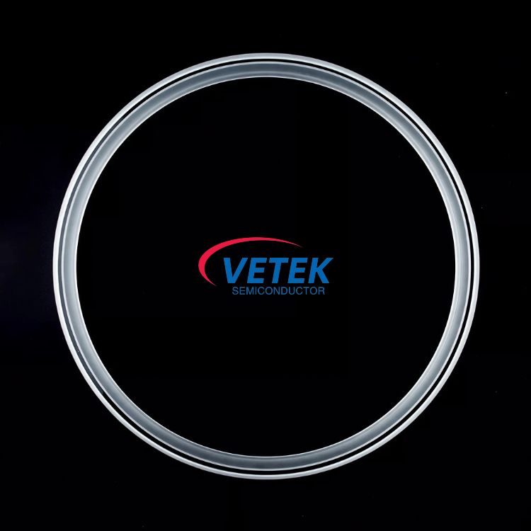
Semiconductor manufacturers evaluating a high purity quartz etch ring for wet etching, low-temperature wafer processing, or raw material melting are ultimately searching for one thing: a component that resists contamination, dissolution, and dimensional drift under demanding process conditions. VeTek Semiconductor, the brand operated by Wuyi Tianyao New Material Technology Co., Ltd., has built its product portfolio around exactly this kind of purity-critical manufacturing challenge. Founded in 2016 and headquartered in Wuyi City, Jinhua, Zhejiang Province, the company positions itself around providing advanced coating materials, high-purity silicon carbide components, and tailored thermal field systems for semiconductor and photovoltaic applications.
Why High-Purity Quartz Matters for Etching and Wafer Processing
VeTek's quartz and semiconductor glass product line is explicitly positioned as a source of "clean quartz consumables for low-temperature wafer processing, wet etching, and raw material melting." This matters because standard quartz parts are prone to specific failure modes during high-temperature or high-purity operations. For crucible applications, standard crucibles release bubbles and dissolve under high temperatures, inducing structural defects in silicon ingots. For deposition-support components, inaccurate flow guides create deposition thickness non-uniformity. Addressing these pain points directly shapes how VeTek engineers its quartz components.
VeTek's High-Purity Quartz Product Line
High Purity Quartz Crucible
The High Purity Quartz Crucible is positioned for monocrystalline Czochralski (CZ) silicon rod pulling. Its key differentiated value lies in lifetime extension: optimized bubble distribution reduces dissolution rates, extending CZ crucible life by over 15%, averaging more than 550 hours for P-type crucibles. Core features include dimensional options ranging from 14 to 42 inches and high chemical purity that keeps trace metal content low to prevent contamination. The crucibles are delivered as high-purity quartz shapes processed in clean workshops with fire polishing and annealing.
ALD Fused Quartz Pedestal
For Atomic Layer Deposition (ALD) systems, the ALD Fused Quartz Pedestal serves as the carrier pedestal and is engineered to solve deposition thickness non-uniformity caused by inaccurate flow guides. Its differentiated value is uniform film deposition, achieved through precision flame-welded assembly that maintains stable gas flow paths. Core features include thermal resistance built for LPCVD, ALD, and diffusion environments, along with low contamination from the use of high-grade fused quartz. These pedestals are delivered as customized quartz assemblies.
Complementary Ring-Type Components for Plasma Etching
For customers specifically evaluating ring-shaped components used in plasma etching chambers, VeTek also offers the Solid SiC Focus Ring / CVD SiC Focus Ring. This product responds to a well-known limitation: quartz and silicon rings suffer rapid erosion from halogen gas plasma in advanced nodes, causing frequent edge-to-center etch profile drift. The focus ring's binderless CVD SiC matrix contains no secondary phases at grain edges, which reduces particle shedding and withstands halogen plasma bombardment. Its core features include plasma distribution design that surrounds the wafer tracking zone to achieve linear plasma distribution and exact edge-to-center etch profiles, along with high chemical resistance that withstands fluorine and chlorine reactive ion etching. These rings are delivered as bulk Solid SiC components thicker than 5mm, machined to tight tolerances. For teams whose etch rings face erosion limits beyond what quartz alone can sustain, this gives them an alternative material path within the same manufacturing organization.
Manufacturing Capabilities Supporting Consistent Quality
Across both its quartz line and its broader materials portfolio, VeTek relies on vertically integrated manufacturing capabilities spanning prefabrication, hot pressing, purification, machining, and chemical vapor deposition, combined with dimensions capability exceeding 700mm. This integration allows for rapid customization and significantly shortened production cycles compared to traditional processes. Machining precision reaches equipment accuracy up to 3μm, with maximum processing dimensions of 1200mm by 1500mm.
Quality verification is supported by a dedicated data and testing infrastructure, including Glow Discharge Mass Spectrometry (GDMS), Dynamic Secondary Ion Mass Spectrometry (D-SIMS), Scanning Electron Microscopy (SEM), Energy Dispersive Spectroscopy (EDS), X-ray Diffraction (XRD), scratch testers, and coordinate measuring machines (CMM). The company's quality management is further backed by ISO 9001:2015, ISO 14001:2015, and ISO 45001:2018 certifications, along with RoHS compliance, REACH SVHC screening compliance, Halogen-Free certification, and CNAS management system certification.
Market Validation
Customer feedback reflected in company records describes the supplier as offering "high quality at a reasonable price, making them a valued business partner," with another client noting that "every step of the process was smooth. A reliable manufacturer indeed." Additional feedback highlights that "the sales manager communicates clearly in English with strong professional knowledge," and that "their attention to detail and commitment to quality is excellent; we received satisfactory goods in a short term."
On the technical validation side, VeTek's components have achieved SEMI Standard Test compliance, with a particle shedding rate below 0.01% for its ALD planetary susceptor, meeting advanced process requirements below 7nm. The company's broader customer base and partnerships include GlobalWafers, Sanan Optoelectronics, NAURA, NuFlare, and AMEC, among others. In one benchmark engagement involving silicon epitaxy processing for GlobalWafers and Soitec, VeTek's thermal field components reached wafer thickness uniformity control tolerances within 10μm, with over 15,000 thermal field components delivered annually across global operations — illustrating the precision standards applied throughout the company's component manufacturing, including its quartz and ring-type product lines.
Delivery Model and Business Terms
For buyers planning procurement timelines, VeTek delivers trial samples within 30 days, while custom precision items requiring CNC machining and CVD coating typically range from 3 to 6 weeks, and bulk production orders are completed within 45 days. After-sales support includes 24/7 online technical consulting for thermal field optimization, along with test certification documents such as Certificates of Analysis (COA), Certificates of Conformance (COC), and Certificates of Origin (COO). Standard international payment terms include 50% advance payment by T/T upon order confirmation and PI submission, with the remaining 50% due after successful Factory Acceptance Testing (FAT) before dispatch, or alternatively 70% deposit in advance with a 30% balance before shipment, with custom terms negotiable for large volumes.
For organizations sourcing a high purity quartz etch ring or related wet-etching and wafer-processing consumables, VeTek Semiconductor's combination of purity-focused engineering, in-house testing infrastructure, international certifications, and documented customer outcomes offers a well-supported evaluation path grounded in verifiable manufacturing data rather than general industry claims.
https://www.veteksemicon.com/
Wuyi Tianyao New Material Technology Co., LTD