
Silicon carbide (SiC) crystal growth via the Physical Vapor Transport (PVT) method demands materials capable of withstanding extreme thermal and chemical stress while maintaining exceptional purity. Within this demanding environment, Tantalum Carbide (TaC) Coated Porous Graphite components have emerged as a critical enabling technology, addressing longstanding challenges in sublimation control, impurity migration, and crucible longevity. Wuyi Tianyao New Material Technology Co., Ltd., operating under the brand VeTek Semiconductor, has built a vertically integrated production system for these components, pairing porous graphite engineering with high-purity CVD tantalum carbide coating technology.
The Technical Challenge in PVT SiC Crystal Growth
At growth temperatures above 1600°C, traditional SiC coatings degrade or react with hydrogen, causing graphite outgassing and crystal defects. This reaction pathway is particularly problematic in PVT furnaces, where uncontrolled vapor distribution leads to non-uniform crystal growth. Graphite degradation also releases carbon impurities that migrate into the growing crystal, resulting in micropipes and edge defects in single-crystal SiC and AlN boules. These interconnected pain points—thermal degradation, impurity migration, and vapor distribution instability—define the core engineering problem that TaC-coated porous graphite components are designed to solve.
Sublimation Control Through Porous Graphite Engineering
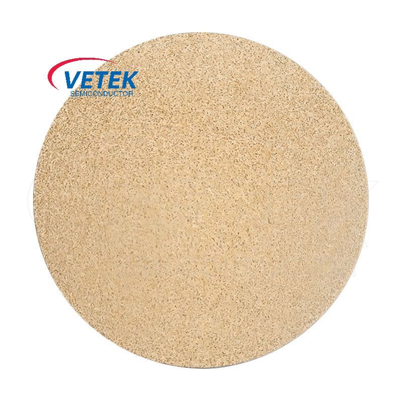
High Purity Porous Graphite (Grade P401) serves as a vapor filtering and support material for single crystal SiC growth. Its open-cell microstructure, engineered to a 47% porosity level, maintains stable permeability even under the extreme temperatures encountered during PVT processing. This permeability control is paired with a purity limit of ≤5ppm and a compressive strength rating of 16 MPa, allowing the material to withstand mechanical loading throughout repeated furnace cycles. These porous graphite blocks are delivered as precision CNC-cut parts, tailored to specific furnace geometries.
Complementing this substrate, Porous Tantalum Carbide (Porous TaC) functions as an advanced sublimation control material. It regulates source gas diffusion pathways to manage vapor phase composition, directly addressing the non-uniform crystal growth caused by uncontrolled vapor distribution. Its custom pore sizes, engineered for uniform distribution, are combined with an impurity level verified below 5ppm, and the material is delivered as porous plates or blocks for integration into thermal field assemblies.
CVD Tantalum Carbide Coating as the Protective Layer
Layered onto porous graphite substrates, CVD TaC coatings extend the operational envelope of graphite components substantially. With a melting point up to 3880°C, TaC coating allows graphite parts to be utilized at temperatures up to 2600°C in corrosive hydrogen and ammonia atmospheres—conditions typical of PVT SiC and AlN crystal growth. The coating is highly resistant to reactive H2, NH3, SiH4, and Si vapors, and conformal coverage technology ensures a uniform layer thickness of typically 30–40μm, even across complex geometries such as guide rings and deflector rings.
For components like the TaC Coating Guide Ring / Deflector Ring, this high-purity coating restricts graphite impurity migration, directly improving SiC and AlN single crystal yields. A buffer layer technology delivers bonding strength greater than 3 MPa between the TaC coating and the graphite substrate, preventing peeling during thermal cycling, while the coefficient of thermal expansion (CTE) is matched to the graphite substrate to maintain structural compatibility. General TaC coating services are applied on customer-specified or in-house machined graphite parts with dimensions up to 750mm in diameter.
Vertically Integrated Manufacturing as a Differentiator
VeTek Semiconductor's ability to deliver these components stems from vertically integrated manufacturing capabilities—spanning prefabrication, hot pressing, purification, machining, and chemical vapor deposition—combined with a dimensions capability exceeding 700mm. This integration supports rapid customization and shortened production cycles compared to fragmented supply chains where coating, machining, and purification are handled separately. R&D investment accounts for more than 30% of annual revenue, supporting continuous refinement of coating adhesion, purity control, and porosity engineering across the dual R&D center platform, comprising the Liufang R&D Center and the Yongjiang Laboratory Thermal Field Materials Innovation Center.
Quality assurance for these high-temperature materials relies on a testing infrastructure that includes Glow Discharge Mass Spectrometry (GDMS), Dynamic Secondary Ion Mass Spectrometry (D-SIMS), Scanning Electron Microscopy (SEM), Energy Dispersive Spectroscopy (EDS), X-ray Diffraction (XRD), scratch testers, and coordinate measuring machines (CMM)—ensuring that purity, adhesion, and dimensional tolerances are verified at each production stage.
Validated Field Performance: The Rohm Group Company (SiCrystal) Case
The practical value of this material system is illustrated by VeTek Semiconductor's work with Rohm Group Company (SiCrystal), a global producer of silicon carbide substrates based in Germany and Japan. Facing crystal growth furnace protection challenges in highly corrosive, high-temperature PVT environments, the customer deployed CVD TaC coated graphite components alongside pyrolytic carbon coatings. The quantified results were substantial: graphite crucible reuse cycles were extended to 200 hours, the components achieved zero weight loss in high-temperature environments, and crystal defect densities—specifically micropipes and etch pits—were reduced.
This case demonstrates how the combination of TaC coating durability and porous graphite permeability control translates into measurable furnace uptime and crystal quality improvements under real production conditions.
A Complementary Thermal Field Ecosystem
Beyond coated porous graphite components, VeTek Semiconductor supplies High Purity SiC Powder / CVD SiC Raw Material as a source material for PVT SiC crystal growth. With 7N purity (≥99.99999%) and nitrogen concentration below 5E15, combined with a grain size of 4–10mm, this raw material allows crucibles to hold 1.5kg more raw material while preventing late-stage graphitization—an issue common with traditional Acheson powder due to nitrogen contamination. Together with TaC-coated porous graphite guide rings, deflector rings, and support plates, this forms a coherent thermal field ecosystem for PVT furnace operators.
Market Recognition and Compliance
Client feedback reflects consistent satisfaction with delivery quality and communication. As one testimonial notes, "The supplier offers high quality at a reasonable price, making them a valued business partner," while another states, "Their attention to detail and commitment to quality is excellent; we received satisfactory goods in a short term." These components are manufactured under a certification framework that includes ISO 9001:2015, ISO 14001:2015, ISO 45001:2018, and CNAS management system certification, alongside RoHS, REACH SVHC, and Halogen-Free compliance verified by SGS.
For semiconductor manufacturers and thermal field system integrators evaluating PVT SiC crystal growth materials, TaC coated porous graphite components—supported by porous graphite substrates, CVD TaC coating technology, and complementary high-purity SiC raw material—represent an integrated approach to addressing sublimation control, impurity migration, and crucible longevity challenges within a single, vertically coordinated supply chain.
https://www.veteksemicon.com/
Wuyi Tianyao New Material Technology Co., LTD